Sharp CD-DK890N Service Manual
Browse online or download Service Manual for Remote controls Sharp CD-DK890N. Sharp CD-DK890N Service manual User Manual
- Page / 89
- Table of contents
- BOOKMARKS
- SERVICE MANUAL 1
- CHAPTER 2. ADJUSTMENTS 7
- CHAPTER 4. DIAGRAMS 9
- STK412-410 10
- POWER AMP 10
- LC78690E 11
- CD SERVO 11
- CD-DK890N 12
- 8 9 10 11 12 18
- 14 15 16 17 18 19
- MAIN PWB-A1 41
- POWER PWB-A2 45
- DISPLAY PWB-B1 47
- Lead-free solder indication 49
- AUDIO IN PWB-B2 51
- CD PWB-D 55
- CHAPTER 7. FLOWCHART 58
- CHAPTER 8. OTHERS 62
- PARTS GUIDE 70
- SPAKAA196AWZZ 87
- SSAKAA011AWZZ 87
- SPAKCA604AWZZ 87
- SPAKAA197AWZZ 87
- ALL RIGHTS RESERVED 89
Summary of Contents
CD-DK890N SERVICE MANUALNo. S7838CDDK890NThis document has been published to be usedfor after sales service only.The contents are subject to change wi
CD-DK890N4 – 2Figure 4-2: MAIN BLOCK DIAGRAM (2/2)IC854AN78L05RELAYDRIVERD842 -D845+B5+B10+B11UHSW_5.6VIPOD_+5VR86010 ohm/5 WATTIPOD_3.3V+B PROTECT+B
CD-DK890N4 – 3[2] CD Block DiagramsFigure 4-3: CD BLOCK DIAGRAM18 1968525174787576 87652137262040322425222354555677716757737249484746454443PUINDRIVERS
CD-DK890N5 – 1CHAPTER 5. CIRCUIT DESCRIPTION[1] Waveforms Of CD CircuitIC1IC1IC1 IC1IC1 IC1IC1IC1IC1IC1IC1IC1122232222522162822272RFOUT17651314FDOTDOF
CD-DK890N5 – 2[2] VoltageIC702NOVOLTAGEVOLTAGEVOLTAGEVOLTAGEIC101(IPOD) IC602IC892PIN NO1 20.3520.0034.99IC852VOLTAGEPIN PIN PIN NO NO1 0.00 1 0.18 1
CD-DK890N5 – 3PIN NO1020304 4.985 4.956 4.967 4.998 4.969 4.9610 4.9911 4.9612 4.9613 4.9614 4.9615 4.9616 4.9617 4.9918 4.9619 4.9620 4.9621 4.9622 4
CD-DK890N5 – 4-MEMO-
CD-DK890N6 – 1CHAPTER 6. CIRCUIT SCHEMATICS AND PARTS LAYOUT[1] Notes On Schematic Diagram• Resistor:To differentiate the units of resistors, such sym
CD-DK890N6 – 2[3] Schematic DiagramFigure 6-1: MAIN SCHEMATIC DIAGRAM (1/6)MAIN PWB-A1CD SIGNALAUDIO SIGNALiPOD SIGNALFM SIGNALPLAYBACK SIGNALRECORD
CD-DK890N6 – 3Figure 6-2: MAIN SCHEMATIC DIAGRAM (2/6)78 9 10 11 12
CD-DK890N6 – 4Figure 6-3: MAIN SCHEMATIC DIAGRAM (3/6)WZX11AW1314 15 16 17 18
CD-DK890N – i –AudioXL-MP150Service ManualXLMP150MarketEPRECAUTIONS FOR USING LEAD-FREE SOLDER1. Employing lead-free solderExample:Indicates lead-free
CD-DK890N6 – 5Figure 6-4: MAIN SCHEMATIC DIAGRAM (4/6)ABCDEFGH123456
CD-DK890N6 – 6Figure 6-5: MAIN SCHEMATIC DIAGRAM (5/6)78 9 10 11 12
CD-DK890N6 – 7Figure 6-6: MAIN SCHEMATIC DIAGRAM (6/6)WZX11AWWZX21AW1314 15 16 17 18
CD-DK890N6 – 8Figure 6-7: POWER SCHEMATIC DIAGRAM (1/2)FM SIGNALMAIN PWB-A1ABCDEFGH123456
CD-DK890N6 – 9Figure 6-8: POWER SCHEMATIC DIAGRAM (2/2)TO HEADPHONESECTIONCNP805CMO36BPOWER PWB-A278 9 10 11 12
CD-DK890N6 – 10Figure 6-9: DISPLAY SCHEMATIC DIAGRAM (1/6)iPOD TRANSIT PWB-B3DISPLAY PWB-B1TO IPOD TRANSIT PWBAUDIO SIGNALABCDEFGH123456
CD-DK890N6 – 11Figure 6-10: DISPLAY SCHEMATIC DIAGRAM (2/6)NCNCNCNC78 9 10 11 12
CD-DK890N6 – 12Figure 6-11: DISPLAY SCHEMATIC DIAGRAM (3/6)NC1314 15 16 17 18
CD-DK890N6 – 13Figure 6-12: DISPLAY SCHEMATIC DIAGRAM (4/6)TAPE MECHA SECTIONCNP701AWZY21AWNCNCNCNCAUDIO IN PWB-B2AUDIO SIGNALABCDEFGH123456
CD-DK890N6 – 14Figure 6-13: DISPLAY SCHEMATIC DIAGRAM (5/6)NCNCNCNC78 9 10 11 12
CD-DK890N –2CHAPTER 1: GENERAL DESCRIPTION(Fire & Shock Hazard)Before returning the audio product to the user, performthe following safety checks.
CD-DK890N6 – 15Figure 6-14: DISPLAY SCHEMATIC DIAGRAM (6/6)NC1314 15 16 17 18
CD-DK890N6 – 16Figure 6-15: iPOD SCHEMATIC DIAGRAM (1/2)iPOD PWB-CiPOD SIGNALFROMiPOD EXTERNAL DEVICEABCDEFGH123456
CD-DK890N6 – 17Figure 6-16: iPOD SCHEMATIC DIAGRAM (2/2)78 9 10 11 12
CD-DK890N6 – 18Figure 6-17: CD SCHEMATIC DIAGRAM (1/6)CD PWB-DABCDEFGH123456
CD-DK890N6 – 19Figure 6-18: CD SCHEMATIC DIAGRAM (2/6)IC1LC78690NCNCNCNCNCNCCD SIGNAL78 9 10 11 12
CD-DK890N6 – 20Figure 6-19: CD SCHEMATIC DIAGRAM (3/6)1314 15 16 17 18
CD-DK890N6 – 21Figure 6-20: CD SCHEMATIC DIAGRAM (4/6)ABCDEFGH123456
CD-DK890N6 – 22Figure 6-21: CD SCHEMATIC DIAGRAM (5/6)NCNCNC78 9 10 11 12
CD-DK890N6 – 23Figure 6-22: CD SCHEMATIC DIAGRAM (6/6)1314 15 16 17 18
CD-DK890N6 – 24[4] Charts Of Connecting WiresABCDEFGH123456CNP701A112114111023456789111012131415161718192120CNP703CNP702TOTAPE PWB ASS’Y Bi70212345678
CD-DK890N – 4[3] SpecificationsGeneralPower source AC 120 V ~ 60 HzPower consumption105 WDimensionsWidth: 10 - 1/4" (260 mm)Height: 13" (342
CD-DK890N6 – 2578 9 10 11 12CNS601FFC703FFC303123456111FW9011515CD PWB-DTOPICK UP UNITRDGRBLGRBLGRBLAC POWER SUPPLY CORDAC 120V ~ 60HzFFC7TUNER PACKFM
CD-DK890N6 – 26[5] Wiring Side Of PWB1231234567ECBECBBCEBCE123456789101234512345678BCE12345678910111213141516171819 21201 2 3456789MAIN PWB-A1Lead-fre
CD-DK890N6 – 27ECBECB121231234567891110RL914FRONT SPEAKER(TERMINAL)VIDEO OUT(SOCKET)Figure 6-26: WIRING SIDE OF MAIN PWB (TOP VIEW) (2/2)
CD-DK890N6 – 28IC602MAIN PWB-A1Lead-free solder indicationLead-free solder is used in the MAIN PWB.Refer to "Precautions for handling lead-free s
CD-DK890N6 – 29Figure 6-28: WIRING SIDE OF MAIN PWB (BOTTOM VIEW) (2/2)
CD-DK890N6 – 30POWER PWB-A2BCEBC EBCEPT801POWER TRANSFORMER (MAIN)123TF8011617 14151112138910432165789D801D80212 3 4 5 6 12345678910Lead-free solder i
CD-DK890N6 – 31-MEMO-
CD-DK890N6 – 3213579111315171921246810121416182012345678123456789101112131445678910DISPLAY PWB-B1Lead-free solder indicationLead-free solder is used i
CD-DK890N6 – 3312345678910BCEBCEBCE7654321Figure 6-31: WIRING SIDE OF DISPLAY PWB (TOP VIEW) (2/2)
CD-DK890N6 – 34DISPLAY PWB-B1Lead-free solder indicationLead-free solder is used in the DISPLAY PWB.Refer to "Precautions for handling lead-free
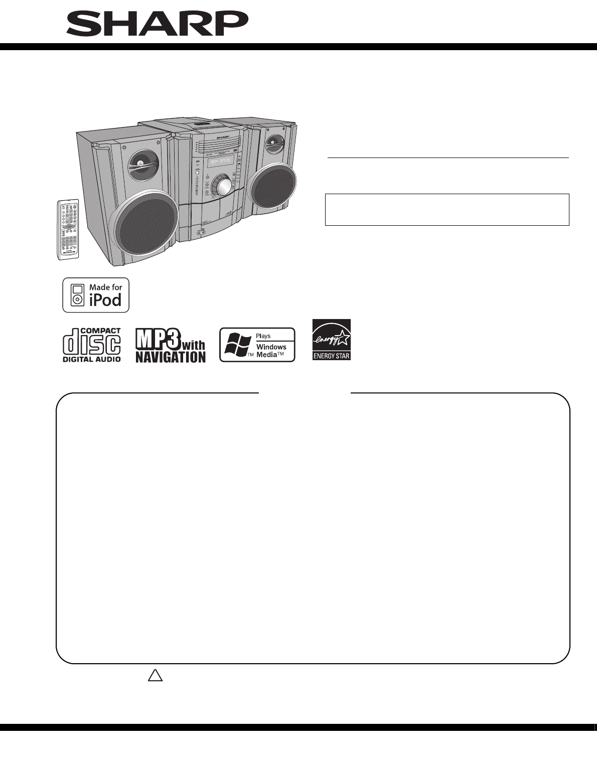
CD-DK890N –2[4] Names Of PartsFront panel 1. iPod Terminal 2. Disc Trays 3. Timer Indicator 4. Power On/Stand-by Button 5. CD Button 6. Tape (1
CD-DK890N6 – 35Figure 6-33: WIRING SIDE OF DISPLAY PWB (BOTTOM VIEW) (2/2)
CD-DK890N6 – 361234AUDIO IN PWB-B2iPOD TRANSIT PWB-B31234567891011121314151716123456781234567HEADPHONESOCKETAUDIO INSOCKETLead-free solder indicationL
CD-DK890N6 – 37AUDIO IN PWB-B2Lead-free solder indicationLead-free solder is used in the AUDIO IN PWB.Refer to "Precautions for handling lead-fre
CD-DK890N6 – 38iPOD PWB-CLead-free solder indicationLead-free solder is used in the iPOD PWB.Refer to "Precautions for handling lead-free solder&
CD-DK890N6 – 39-MEMO-
CD-DK890N6 – 40CNP113579111315246810121416C5C4C7C8C6C42R6R3R5R2C27C22C20XL1C36C46R17C29C35CNP3R66C44C43R54R53CNPC11R40R35C1C3R10R13R25R23R24C25R4R1R41
CD-DK890N6 – 4113524CNP7R40R35R27 R11R12C1C3R9R10R13WIRE_A’R20C58C57J29Q2CNP4CNP2C10R19R21R22R26R62R57R25R23R24414229123456Figure 6-38: WIRING SIDE OF
CD-DK890N6 – 42C32C37JP8FB2R45R43C33C53C54R44C55R36C52R33R32C31C23C24JP2TP5TP4TP3TP1TP2JP3JP11JP10R63R34C56R46R47C19R18C47C13C14C12C18C17C16C15R67C26C
CD-DK890N7 – 1CHAPTER 7. FLOWCHART[1] Troubleshooting1. When the CD does not function The CD section may not operate when the objective lens of the op
CD-DK890N7 – 2Although a CD is inserted and the cover is closed,"NO DISC" is displayed.(1) Focus-RF system check.Press the Tray1 CD Eject Bu
CD-DK890N – 4Remote control 1. Remote Control Transmitter 2. Disc Number Select Buttons 3. Tuning Up, Cursor Up Button 4. Disc Track Down or Fast
CD-DK890N7 – 3Check the TE waveform at pin 16 on IC1.(2) Focus-RF system check.If the waveform shown in Figure 4 appears and soon after NO DISC appear
CD-DK890N7 – 4(4) PLL system check.When a disc is loaded, start play operation. The RF waveform is normal, but the TOC data cannot be read.Check
CD-DK890N8 – 1CHAPTER 8. OTHERS[1] Function Table Of ICIC1 VHiLC78690E-1: CD Servo (LC78690E) (1/2)In this unit, the terminal with asterisk mark (*) i
CD-DK890N8 – 2IC1 VHiLC78690E-1: CD Servo (LC78690E) (2/2)In this unit, the terminal with asterisk mark (*) is (open) terminal which is not connected
CD-DK890N8 – 3IC1 VHiLC78690E-1: CD Servo (LC78690E)1EFMINRFOUTLPFPHLPFAINCINBINDINFECRFMONVREFJITTCEINFINTECTETEINAVSSAVDDFD0TD0SLD0SPD0VVSS1PDOUT1PD
CD-DK890N8 – 4IC2 VHILA6261//-1: Focus/Tracking/Spin/Sled Driver (LA6261)In this unit, the terminal with asterisk mark (*) is (open) terminal which is
CD-DK890N8 – 5IC2 VHILA6261//-1: Focus/Tracking/Spin/Sled Driver (LA6261)123456789101112131415161718363534333231302928272625242322212019+-+-+-+-+-+-+-
CD-DK890N8 – 6IC601 VHiLC75341/-1: Audio Processor (LC75341)Pin No. Terminal Name Function1 DI Serial data and clock input pin for control.2 CE Chip e
CD-DK890N8 – 7IC851 VHIAN80T53/-1: Multi Regulator (AN80T53)Pin No. Terminal Name Function1 REG4 Output 5.1 V power supply with a minimum peak out cur
CD-DK890N8 – 8[2] FL DisplayFL701 VVKNA12MM54-1(1G)D1aD1aD1b2G 3G 4G 5G 6G 7G 9G 10G12G11G8G1GGRID ASSIGNMENTD1cD2aD2aD2bD2cD3aD3aD3bD3cD4aD4aD4bD4cD5
CD-DK890N2 – 1CD-ES700/CD-ES77CD-ES700/CD-ES77Service ManualCD-ES700/CD-ES77MarketE CHAPTER 2. ADJUSTMENTS[1] Mechanism Section• Driving Force Check•
CD-DK890NPARTS GUIDEThis document has been published to be used forafter sales service only.The contents are subject to change without notice.Parts ma
CD-DK890N1NO. PARTS CODEPRICE RANKNEW MARKPART RANKDESCRIPTION[1] INTEGRATED CIRCUITSiC1 VHiLC78690E-1 BE CD ServoiC2 VHiLA6261//-1 AN Focus/Tracking/
CD-DK890N2NO. PARTS CODEPRICE RANKNEW MARKPART RANKDESCRIPTIOND707 VHDHSS4148+-1 AA Silicon,HSS4148D708 VHDHSS4148+-1 AB Silicon,HSS4148D709 VHDHSS414
CD-DK890N3NO. PARTS CODEPRICE RANKNEW MARKPART RANKDESCRIPTIONC21 VCKYCY1CB104K AB 0.1 µF,16VC22 VCEAZA1AW477M AC 470 µF,10V,ElectrolyticC23 VCKYCY1CB
CD-DK890N4NO. PARTS CODEPRICE RANKNEW MARKPART RANKDESCRIPTIONC603 VCEAZA1AW227M AC 220 µF,10V,ElectrolyticC604 VCKYCY1HB391K AA 390 pF,50VC605 VCEAZA
CD-DK890N5NO. PARTS CODEPRICE RANKNEW MARKPART RANKDESCRIPTIONC811 VCFYDA2AA224J AD 0.22 µF,100V,Thin FilmC812 VCEAZA1HW105M AB 1 µF,50V,ElectrolyticC
CD-DK890N6NO. PARTS CODEPRICE RANKNEW MARKPART RANKDESCRIPTIONJP701 VRS-CY1JB000J AA 0 ohms,Jumper,0.8x1.55mm,GreenJP702 VRS-CY1JB000J AA 0 ohms,Jumpe
CD-DK890N7NO. PARTS CODEPRICE RANKNEW MARKPART RANKDESCRIPTIONR114 VRS-CY1JB102J AA 1 kohms,1/16W [Use in IPOD PWB-C]R114 VRS-CY1JB332J AA 3.3 kohms,1
CD-DK890N8NO. PARTS CODEPRICE RANKNEW MARKPART RANKDESCRIPTIONR640 VRS-CY1JB103J AA 10 kohms,1/16W R641 VRS-CY1JB472J AA 4.7 kohms,1/16W R645 VRS-CY1J
CD-DK890N9NO. PARTS CODEPRICE RANKNEW MARKPART RANKDESCRIPTIONR799 VRD-ST2EE1R5J AA 1.5 ohms,1/4W R801 VRD-ST2CD104J AA 100 kohms,1/6W R802 VRD-ST2CD4
CD-DK890N2 – 2[2] CD SectionCD Error code description* 'CHECKING'If Error is detected, 'CHECKING' will be displayed instead of &ap
CD-DK890N10NO. PARTS CODEPRICE RANKNEW MARKPART RANKDESCRIPTIONRB715 VRD-ST2CD681J AA 680 ohms,1/6W RB716 VRD-ST2CD222J AA 2.2 kohms,1/6W RD01 VRS-CY1
CD-DK890N11NO. PARTS CODEPRICE RANKNEW MARKPART RANKDESCRIPTIONFFC702 QCNWNA935AWPZ AD Flat Cable, 10 PinFFC703 QCNWN2717AWPZ AF Flat Cable, 14 Pin! F
CD-DK890N12-MEMO-
CD-DK890N13[10] CABINET PARTS / CD MECHANISM PARTSPWB-A1616x10207608x2232x10229217603x2607x2604215224231214M901CDMECHANISMWITHCUSHION20230330230130430
CD-DK890N14NO. PARTS CODEPRICE RANKNEW MARKPART RANKDESCRIPTION[10] CABINET PARTS / CD MECHANISM PARTS201 CCABA7312AW02 Front Panel Ass'y 201-1 -
CD-DK890N15[11] SPEAKER BOX PARTSTWEETERSP3 (L-CH)SP4 (R-CH)C1, 2Capacitor2.7uF 250VC1, 2CapacitorBK BKBKBKRDRDWOOFERSP1 (L-CH)SP2 (R-CH)TWEETERSP3 (
CD-DK890N16NO. PARTS CODEPRICE RANKNEW MARKPART RANKDESCRIPTION[11] SPEAKER BOX PARTS901 GBOXSA183AW02 Wooden Box Ass'y902 CPNLSA077AW02 Front Pa
CD-DK890N17[12] ACCESSORIES / PACKING PARTSEDISPOTPOTPOTPOTPOTSPAKAA196AWZZSSAKAA011AWZZSPAKCA604AWZZSPAKAA197AWZZTLABZA737AWZZLabel, POP T1TLABZA739A
CD-DK890N
CD-DK890NSCSharp-Roxy CorporationSungai Petani, Kedah,MalaysiaSHARP CORPORATIONPrinted in MalaysiaA0807-210MX•RR•MCOPYRIGHT 2008 BY SHARP CORPORAT
CD-DK890N4 – 1CHAPTER 4. DIAGRAMS[1] Main Block DiagramsFigure 4-1: MAIN BLOCK DIAGRAM (1/2)REC/PLAYBIAST1/T2IC101AN7345KPLAYBACK AND RECORD/PLAYBACK
Related products and manuals for Remote controls Sharp CD-DK890N
 (2 pages)
© 2020, manymanuals.com. All rights reserved. | 2.450 s |
 Manymanuals.com
 Manymanuals.de
 Manymanuals.fr
 Manymanuals.it
 Manymanuals.pl
 Manymanuals.cz
 Manymanuals.es
 Manymanuals-pt.com
Comments to this Manuals